GESP TECHNOLOGY
PRINTED CIRCUIT BOARD MANUFACTURING CAPABILITIES
Introduction
Our PCB capabilities to meet customers ’ manufacturing requirements. and our supply chain has a variety of procurement and production processes. GESP Tech can offer competitive prices . because the PCB capabilities has been fully integrated into the standard production system. GESP Tech PCB Capabilities can provide our clients with the most professional services. whether it is standard PCB production or multi-layer Advanced PCB. Prenatal document testing is free, as is the full set of electronic experimentation. It is simple to contact GESP Tech. Call +86-0411-8853-5976 or email marketing@guestforeal.com. and the sales engineer best-suited to the nature of your inquiry will contact you within 24 hours.
PRINTED CIRCUIT BOARD MANUFACTURING CAPABILITIES
| Feature | Capability | |
| Layer Count | 1-6Layers | |
| Material | PI, PET, PEN, FR-4 | |
| Final Thickness | 0.002″ – 0.1″ (0.05-2.5mm) | |
| Surface Treatment | Lead-free: ENG Gold; OSP, Immersion silver, Immersion Tin | |
| Max / Min Board Size | Min: 0.2″x0.3″ Max: 20.5″x13″ | |
| Min Trace Width | 0.5oz: 4/4mil | |
| Min Clearance Inner | 1oz: 5/5mil | |
| 2oz: 5/7mil | ||
| Min Trace Width | 1/3oz-0.5oz: 4/4mil | |
| Min Clearance Outer | 1oz: 5/5mil | |
| 2oz: 5/7mil | ||
| Min Hole Ring Inner | 0.5oz: 4mil | |
| 1oz: 5mil | ||
| 2oz: 7mil | ||
| Copper Thickness | 1/3oz – 2oz | |
| Max / Min Insulation Thickness | 2mil/0.5mil (50um/12.7um) | |
| Min Hole Size&Tolerance | Min hole: 8mil | |
| Tolerance: PTH±3mil, NPTH±2mil | ||
| Min Slot | 24mil x 35mil (0.6×0.9mm) | |
| Silkscreen Line Width | 5mil | |
| Gold Plating | Nickel: 100u” – 200u” | Gold: 1u”-4u” |
| Immersion Nickel / Gold | Nickel: 100u” – 200u” | Gold: 1u”-5u” |
| Immersion Silver | Silver: 6u” – 12u” | |
| OSP | Film: 8u” – 20u” | |
| Test Voltage | Testing Fixture: 50-300V | |
| Profile Tolerance of Punch | Accurate mould: ±2mil | |
| Ordinary mould: ±4mil | ||
| Knife mould: ±8mil | ||
| Hand-Cut: ±15mil | ||
Why choose GESP
RELIABLE AND TRUSTWORTHY PCB MANUFACTURER
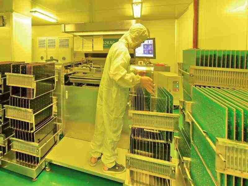
Our PCB factory includes a 57,000-square-meter workshop, with 400 staff, and a monthly manufacturing capacity of 65,000 square meters.At the same time, Our factory is approved by ISO9001-2008,ISO14001:2004,IATF16949,UL, RoHS, etc.As well as that our featured to consist of 2-6 layer boards, and GESP offer a rapid turnaround for prototypes and small quantities. Also from simple single and double panels to complicated high-tech circuit boards, we’ve been pushing the envelope.
GESP TECH RELIABLE PCB MANUFACTURER IN CHINA
TALK ABOUT YOUR PROJECT NOW!
[contact-form-7 id=”4073″ title=”GENERAL USE”]