GESP TECH -TRUSTWORTHY ONE-STOP PCB SERVICES
STREAMLINING THE PCB PRODUCTION PROCESS
FOR HIGHER EFFICIENCY
Introduction
The design engineer assigns each circuit board a unique function. In order to produce a PCB that is adequate for achieving this function. it is necessary to use a complex manufacturing procedure. Consequently, the PCB production process is a multistep, complex procedure. This review focuses on the most vital procedures involved in the fabrication of a multilayer PCB. When purchasing PCBs from GESP Technology, you are investing in quality that will pay for itself over time. we ensured product quality by control the PCB production process strictly. thereby ensuring that the product fulfills its claims.
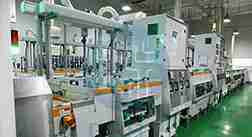
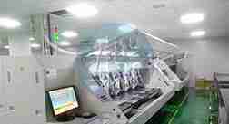
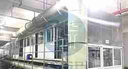
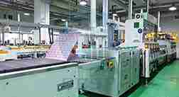
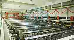
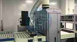
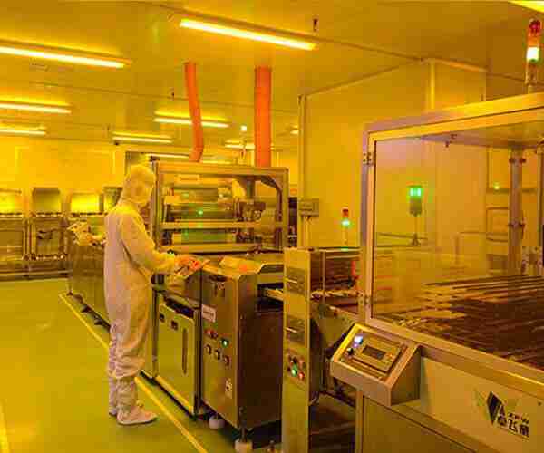
MASS PCB PRODUCTION PROCESS
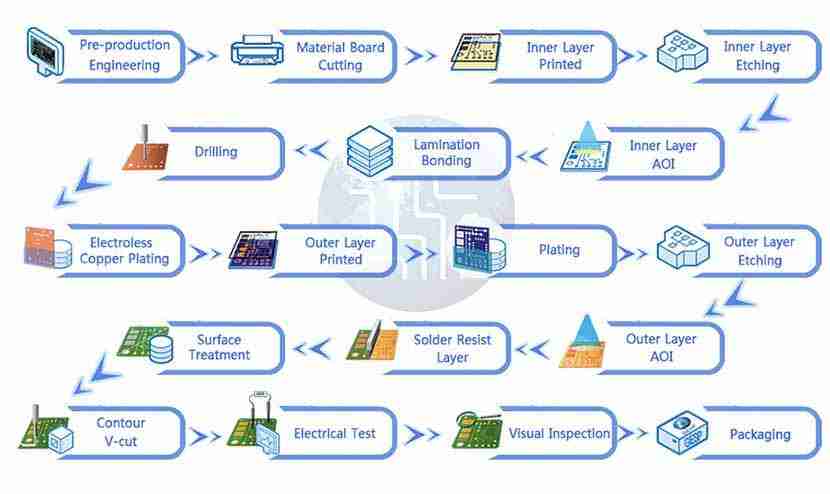
GESP CAPABILITITIES PCB PRODUCTION PROCESS
Design and Output
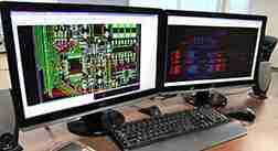
Check the Gerber file provided by the customer . and generate the layers of Conductive Pattern, Drilling, Solder Mask, Silkscreen’s Artwork Master etc.
Material Board Cutting
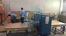
According to the customer’s specifications. the copperclad PCB’s corresponding material is cut to a size . suitable for the PCB manufacturing process.
Inner Layer Printed
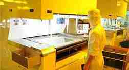
The image transferred to the surface of the board using photosensitive dryfilm and UV light. which polymerizes the dry film exposed by the artwork.
Exposure

Etch copper off the panel. After removing this copper, the dry coating is removed. leaving the design-matching copper circuitry.
Circuit Check
Check the developed circuit .GESP Technology does not allow open circuits
Inner Eaching

Use CuCl2 to etch away the copper without the protective layer
Inner Layer AOI
Use the principle of optical reflection to detect the adbsence of lines.
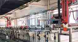
Brown & Lamination
Brown the circuit boards of each layer fix the stacked boards in order.
Drilling
Driliing vias for layer-to-layer line connection
Copper Plating
Via hole is deposited with 20-40μ ,and a layer of 200-500μ copper is electroplated to protect the copper layer
Outer Layer Image
Like the inner layer imaging process the outer circuit layer is formed through dry film
Pattern Plating
Thicken the exposed copper suface to the thickness required by the customer
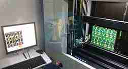
Outer Layer AOI
Check the integrity of the outer circuit
Solder Mask
The solder resist ink is printed on the board with a screen.This process will undergo the process of exposure development, exposing the parts that need to be soldered
Legends Printing
Print the characters on the PCB surface and bake until the characters are hardened
Surface Treatment
Surface treatment is made a protective layer formed on the surface of the copper layer to prevent oxidation if the copper surface.
CNC Routing & V-Cut
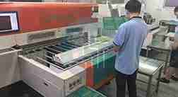
This process will cut the PCB into the size and shape required by
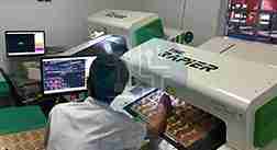
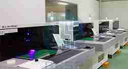
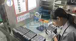
Electrical Test
GESP Technology uses universal on grid and moving probe to test the electrical performance of the PCB
Visual Inspection
Final inspection of PCB dimensions board thickness line width,aperture,solderability,etc.
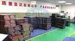
PCB Packing
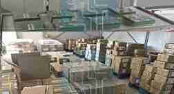
GESP Technology vacuum-packs the tested PCBs, put them together with a desiccant. then, put them in our carton,ensure that the PCB reaches the customer in the best condition.
RELIABLE PCB FABRICATION MANUFACTURER
As we konw ,GESP has more than 25 years experience with 2 Layer PCB,multilayer PCB prototypes. At the sam time , PCB production, PCB Fabrication, and PCB assembly also our strong item. Becasue of Our PCB manufacturing team ensures that all design, development, quality, cost, inspection, turnaround. and delivery requirements of our PCB customers are met. As a result, For specific capacity requirements for the production of bulk PCB prototypes. high/low volume PCB assembly. and low-cost printed circuit board prototypes, please submit a PCB Quote request. Certainly, We have different printed circuit board quote request forms for different needs. such as PCB Layout quote, Printed circuit board fab quote, PCB Prototype quote. PCB assembly quote, PCB Material management quote, PCB turnkey assembly quote. or for any custom PCB assembly quote, please contact us . and our PCB Expert technician will make sure to understand your specifications.
Client's Love PCB Manufacturer in China
TALK ABOUT YOUR PROJECTS NOW!
[contact-form-7 id=”4073″ title=”GENERAL USE”]